Multilayer and high-layer PCBs up to 64 layers
From four-layer controllers to thick backplanes, multilayer boards make up most of our volume. We laminate up to 64 layers, drill through-holes at a 25:1 aspect ratio and plate them evenly on pulse plating lines.
For signal integrity we control impedance, back-drill stubs and build hybrid stacks with low-loss materials. Multilayer prototypes ship from 24 hours.
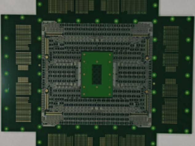
Multilayer capability
| Layer count | 4–64 (34 shipped) |
|---|---|
| Board thickness | 0.2–6.5 mm (6.35 mm shipped) |
| Aspect ratio | 25:1 (shipped) |
| Minimum mechanical drill | 0.10 mm |
| Trace / space | 2/2 mil (0.05 mm) |
| Copper weight | 1/3–8 oz |
| Impedance control | ±10% |
| Back-drill | Yes |
| Maximum panel | 609 × 889 mm |
| Materials | FR-4 Tg 130–180, IT-180, TU872, hybrid with PTFE |
Built for thick, dense boards
Pulse plating for deep holes
Pulse plating keeps copper thickness even down the barrel of a 25:1 hole, which is what fails first on thick boards.
Resin plugging
Through-holes and via-in-pad are plugged with resin and capped so you can place components directly on top.
Controlled impedance
Our engineers model your stack-up before production and adjust trace widths to meet target impedance, with impedance test coupons on the production panel.
26 CNC drills, 27 flying probes
Drilling and electrical test both run in-house on our own machines.
Typical uses
- Servers and storage
- Telecom and 5G base stations
- Semiconductor test boards
- Industrial controllers
- Graphics cards
- Aerospace and defense electronics
Maximum values are individual process limits, not a promise that every limit can be combined. A 34-layer, 7-step HDI board is a documented delivered build; projects above this layer count require engineering review.
Explore the builds →HSX / Our factory
The equipment behind the specification.
Original photographs from our Shenzhen factory. Explore the manufacturing process and the equipment used to build and inspect your boards.
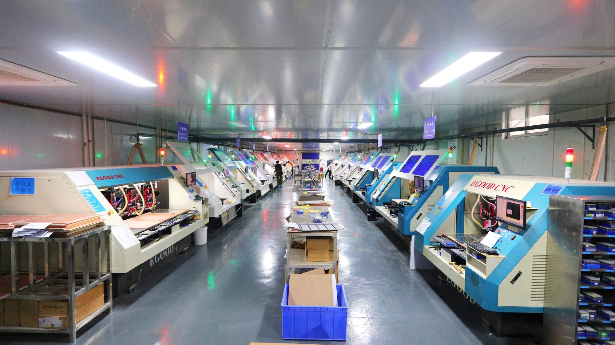
CNC drilling
Mechanical drilling produces through-holes and defined drill structures. Our drilling workshop supports prototypes and production orders.
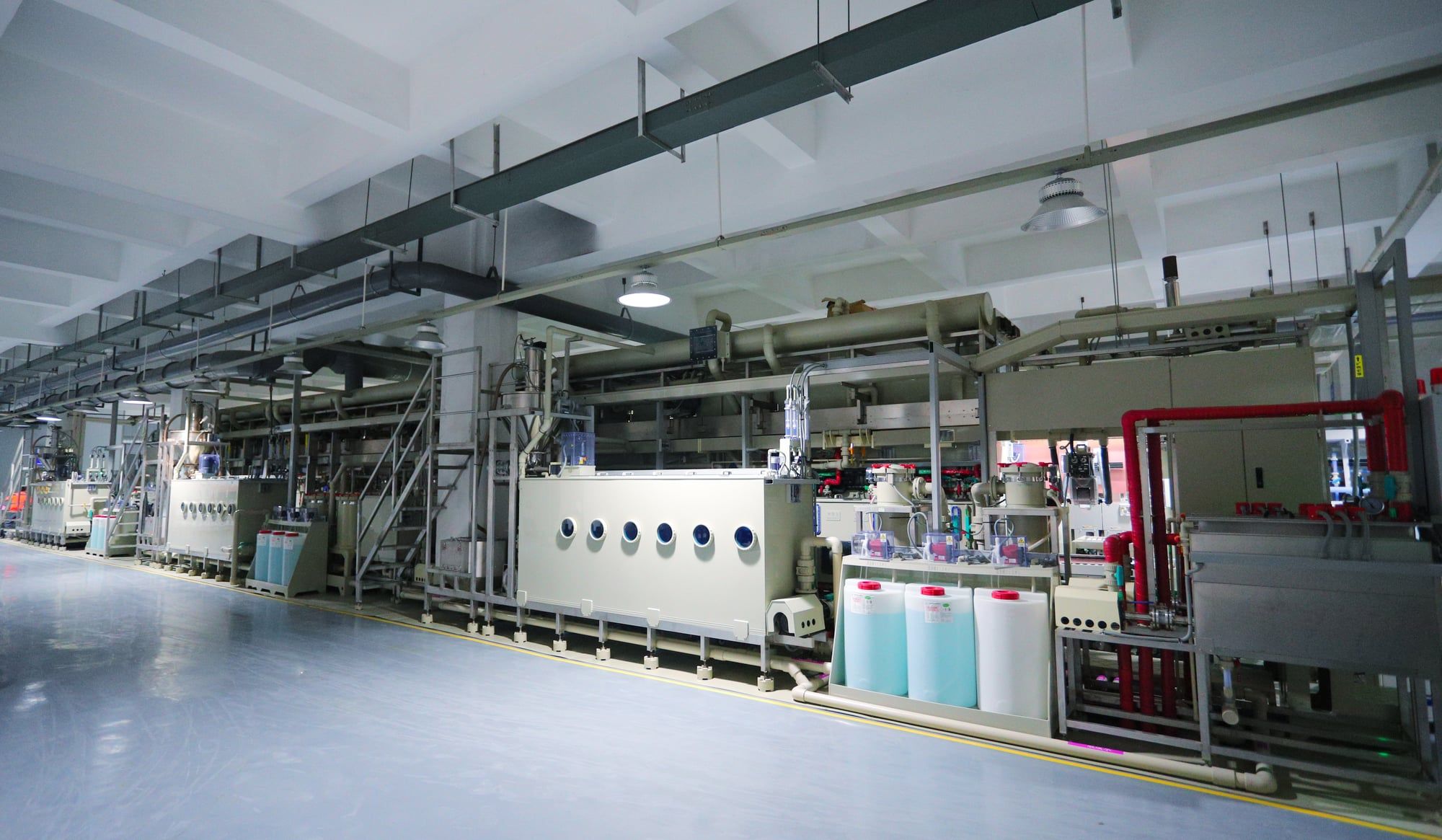
VCP copper plating
Continuous plating equipment supports the copper deposition and via-fill processes used in PCB manufacture.
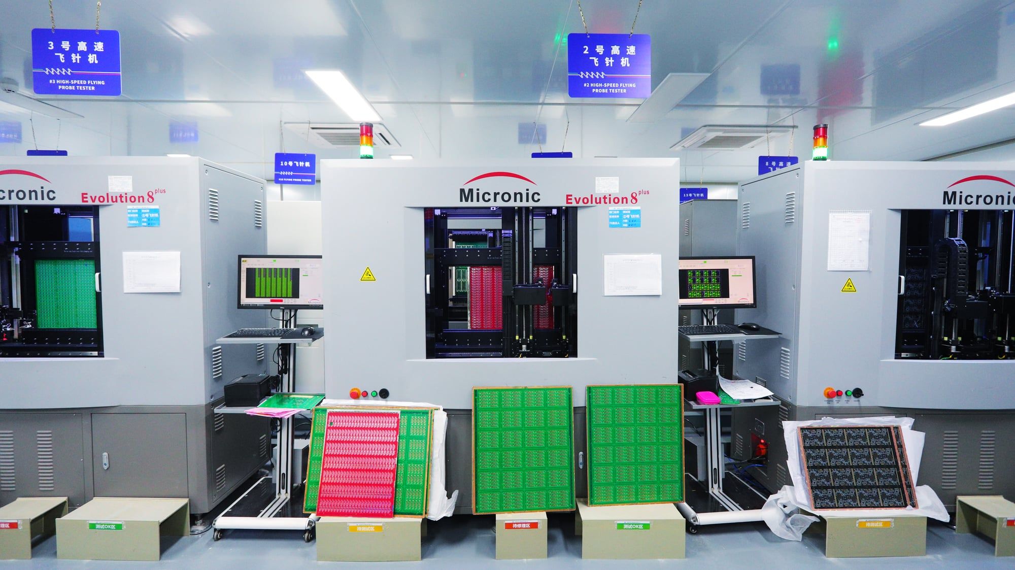
High-speed flying-probe testing
Flying-probe equipment tests continuity and isolation without a dedicated fixture, supporting prototypes and complex board designs.
Questions engineers ask us
What is the maximum layer count you build?
Up to 64 layers. Our deepest shipped HDI build has 34 layers with seven lamination steps; plain multilayer boards above that are quoted after a stack-up review.
What aspect ratio can you plate?
Up to 25:1, board thickness to drill diameter, proven on a 6.35 mm, 34-layer board we shipped.
Do you offer impedance control and test reports?
Yes. We control impedance to ±10% as standard and can supply impedance test reports from coupons on the production panel.
How long does a 12-layer prototype take?
Quick-turn 12-layer prototypes start at 4 days. Standard prototypes take about 10 days, and production orders 19–20 days.
Send your design. Let’s build it properly.
Upload Gerber or ODB++, stack-up and quantities. Standard PCB quotes usually take 30 minutes in working hours; HDI, rigid-flex and special materials usually take up to 24 hours.