HDI PCBs, from 1-step to any-layer
HDI is where we started and where most of our engineering effort goes. We build blind and buried microvia boards from one to seven sequential lamination steps, and any-layer structures where every layer is connected by copper-filled laser vias.
Our deepest shipped build has 34 layers and seven lamination steps at 6.35 mm. Most HDI work is smaller than that: phone and wearable mainboards, camera modules, fine-pitch BGA breakouts and LED display boards.
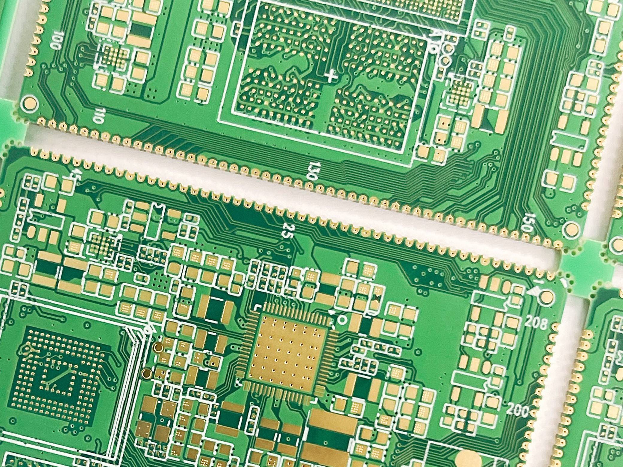
HDI capability
| Structure | 1+N+1 to 7+N+7, any-layer |
|---|---|
| Microvias | Stacked or staggered, copper-filled by VCP |
| Minimum laser via | 0.10 mm (4 mil) |
| Minimum mechanical drill | 0.10 mm |
| Trace / space | 2/2 mil (0.05 mm) |
| BGA pitch | 0.4 mm |
| Via-in-pad | Resin plugged and capped (VIPPO) |
| Layer count | Up to 64 (34-layer, 7-step shipped) |
| Materials | FR-4 Tg 150–180, IT-180, TU872, halogen-free |
| Imaging | LDI for inner layers, outer layers and solder mask |
How we build HDI
Laser drilling and VCP via fill
Microvias are laser drilled, desmeared by plasma and filled in a Dongwei vertical continuous plating line, so stacked vias land on flat copper.
LDI on every imaging step
Seven LDI imagers handle inner layers, outer layers and solder mask. No film shrink, and registration holds across repeated laminations.
X-ray target drilling
After each lamination an X-ray drill locates inner targets before the next build-up, keeping layer-to-layer registration within tolerance.
Engineering review before production
Our CAM engineers check stack-up, via structure and DFM before quoting. Quick-turn jobs get engineering questions the same day.
Typical applications
- Smartphone and wearable mainboards
- Camera and sensor modules
- Fine-pitch LED display
- Graphics and computing
- Drones and UAV flight controllers
- Automotive ADAS modules
Maximum values are individual process limits, not a promise that every limit can be combined. A 34-layer, 7-step HDI board is a documented delivered build; projects above this layer count require engineering review.
Explore the builds →HSX / Our factory
The equipment behind the specification.
Original photographs from our Shenzhen factory. Explore the manufacturing process and the equipment used to build and inspect your boards.
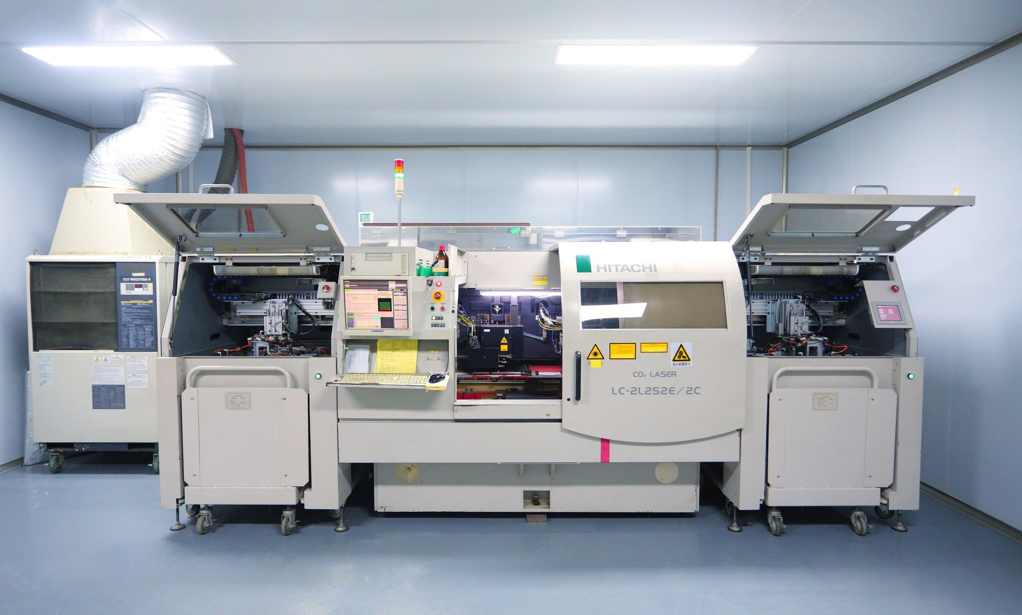
Laser drilling
Laser equipment forms the microvias used in HDI structures. Via spans and stacked or staggered construction are reviewed against the stack-up.
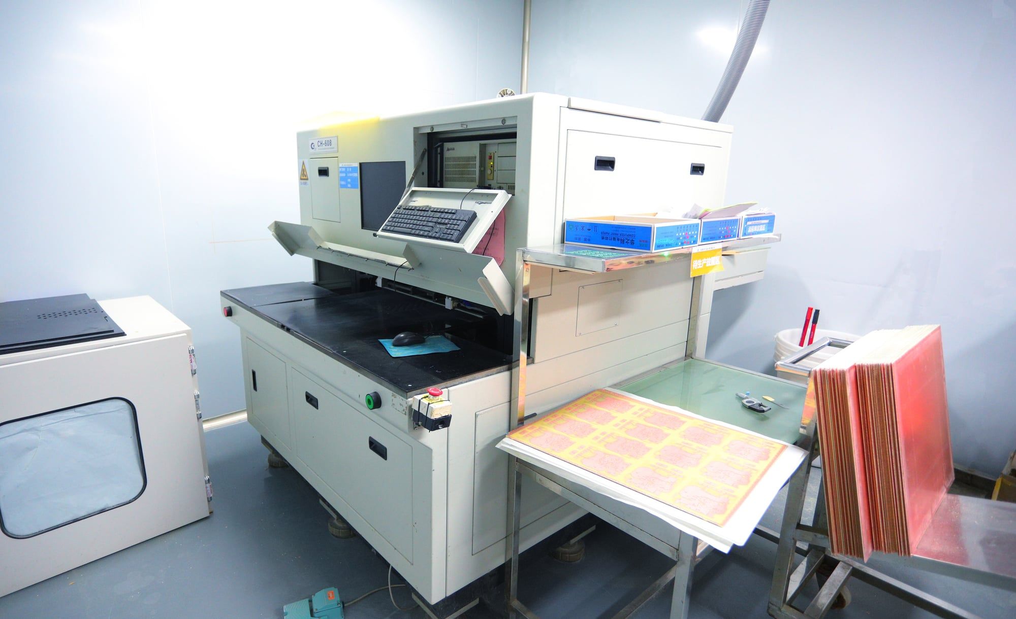
X-ray target drilling
X-ray target location supports layer registration after lamination, before subsequent drilling and build-up operations.
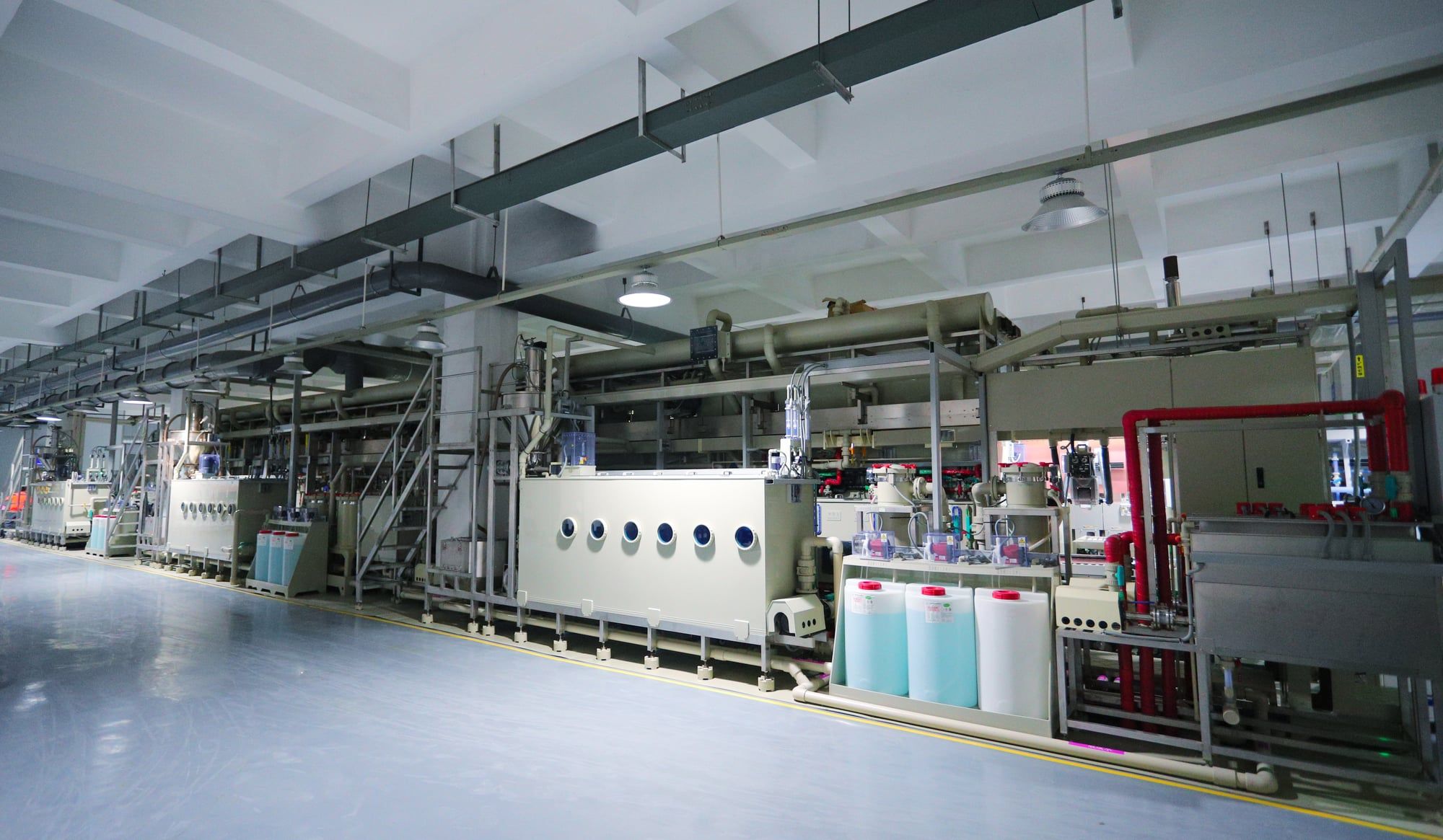
VCP copper plating
Continuous plating equipment supports the copper deposition and via-fill processes used in PCB manufacture.
Questions engineers ask us
What is the difference between 1-step, 2-step and 3-step HDI?
The step count is the number of sequential laminations after the core. A 1-step (1+N+1) board has one microvia layer on each side; a 3-step (3+N+3) board has three, built and laminated one at a time. More steps allow finer BGA breakout but add lamination cycles, cost and lead time.
Do you build stacked or staggered microvias?
Both. Stacked microvias are copper-filled so the next via lands on a flat pad. Staggered vias are offset by one pad and are a little cheaper and more forgiving. We recommend staggered when your layout allows it.
How fast can you build an HDI prototype?
Quick-turn HDI starts at 72 hours for 1-step prototypes up to 1 m². Standard HDI prototypes take 11–18 days depending on layer count and steps.
Can you do any-layer HDI?
Yes. Any-layer boards use copper-filled laser vias between every pair of layers instead of mechanical through-holes. Send us the stack-up and we will confirm material and lamination sequence before quoting.
What files do you need for an HDI quote?
Gerber RS-274X or ODB++, an NC drill file per drill span, a stack-up drawing that shows each microvia span, and a fabrication note with material, finish, impedance and quantity.
Send your design. Let’s build it properly.
Upload Gerber or ODB++, stack-up and quantities. Standard PCB quotes usually take 30 minutes in working hours; HDI, rigid-flex and special materials usually take up to 24 hours.