RF, microwave and high-speed PCBs
For RF and high-speed digital boards the laminate is part of the circuit. We build on Rogers, PTFE and low-loss FR-4-class materials such as TU872 and IT-180, either alone or in hybrid stacks that put expensive material only where the signals need it.
Our method for multilayer high-frequency boards is protected by Chinese invention patent CN119300231B.
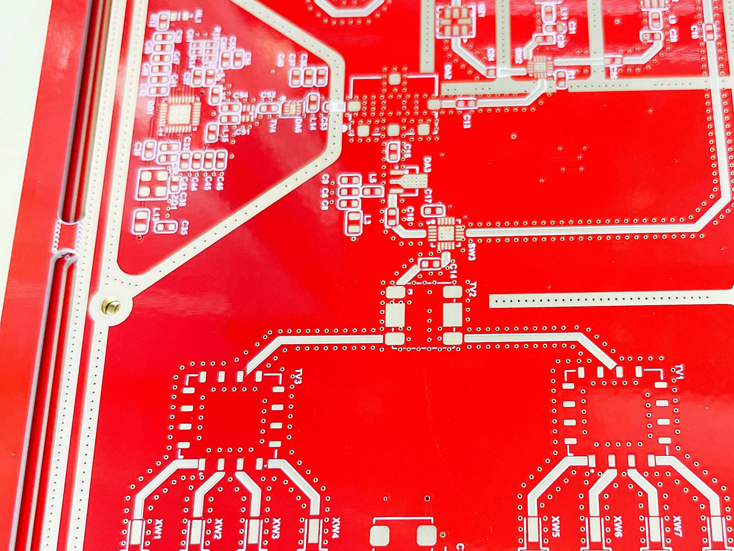
RF and high-speed capability
| Materials | Rogers, PTFE, TU872, IT-180, ceramic-filled |
|---|---|
| Hybrid stacks | 2–20 layers (PTFE + FR-4) |
| Impedance control | ±10% |
| Back-drill | Yes |
| Trace / space | 2/2 mil (0.05 mm) |
| Finish | ENIG, immersion silver, immersion tin, hard gold |
| Patent | CN119300231B, multilayer high-frequency PCB and preparation method |
Getting RF boards right
PTFE hole preparation
Plasma treatment activates PTFE hole walls so copper bonds reliably. It is the step that most often fails at shops that do not run PTFE regularly.
Hybrid lamination
Mixing PTFE and FR-4 in one stack needs matched press cycles. We build hybrid stacks up to 20 layers.
Etch compensation
Line width on RF layers is compensated per material and copper weight so transmission lines land on target.
Typical uses
- 5G and telecom radios
- Antennas and RF front ends
- Radar and automotive sensors
- Satellite and microwave links
- High-speed backplanes and servers
Maximum values are individual process limits, not a promise that every limit can be combined. A 34-layer, 7-step HDI board is a documented delivered build; projects above this layer count require engineering review.
Explore the builds →HSX / Our factory
The equipment behind the specification.
Original photographs from our Shenzhen factory. Explore the manufacturing process and the equipment used to build and inspect your boards.
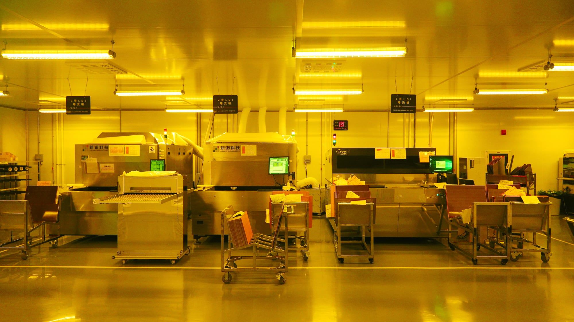
LDI imaging
Direct imaging transfers fine circuit patterns onto the panel. Inner-layer, outer-layer and solder-mask exposure are covered by our LDI equipment.
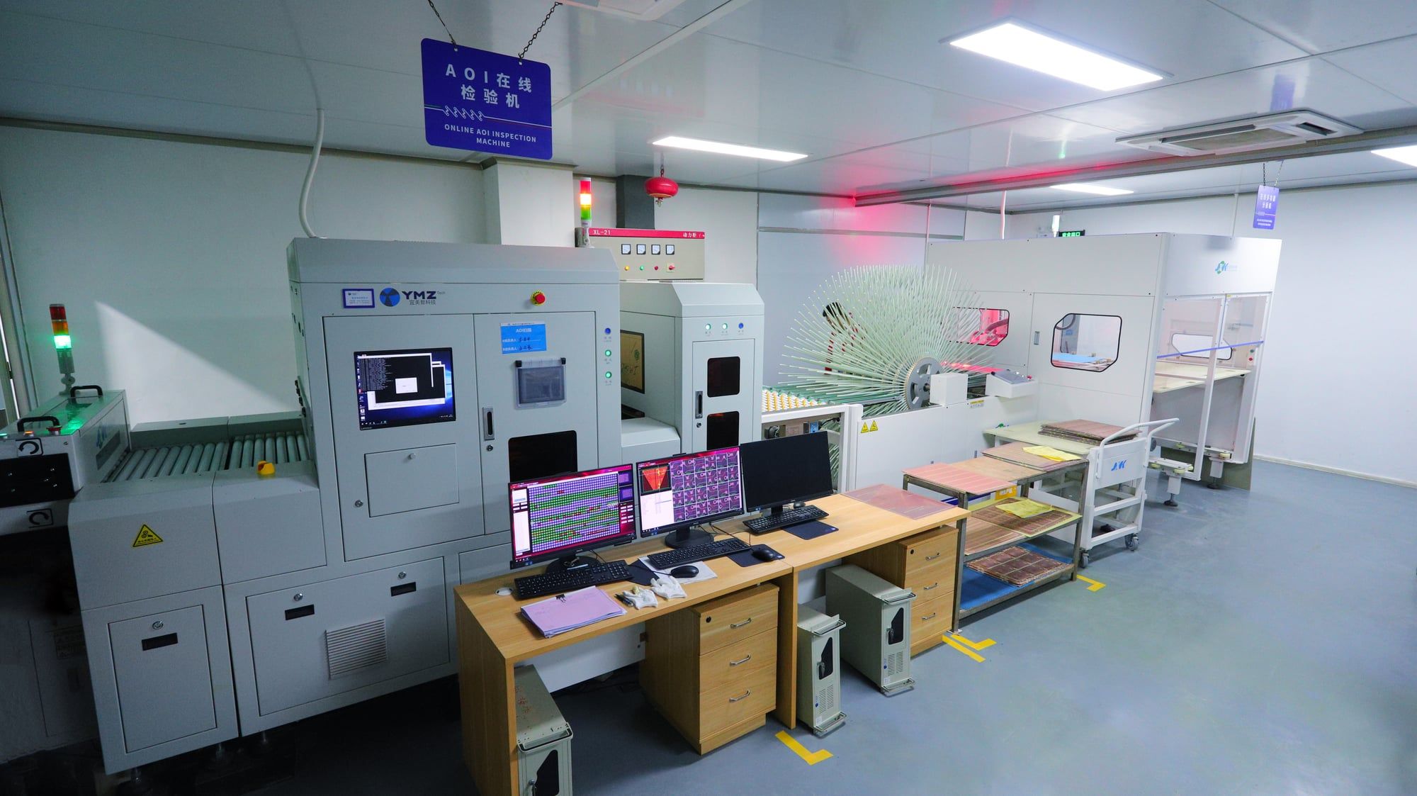
Automatic optical inspection
AOI checks circuit patterns during fabrication. Detected features are reviewed before boards continue through the process.
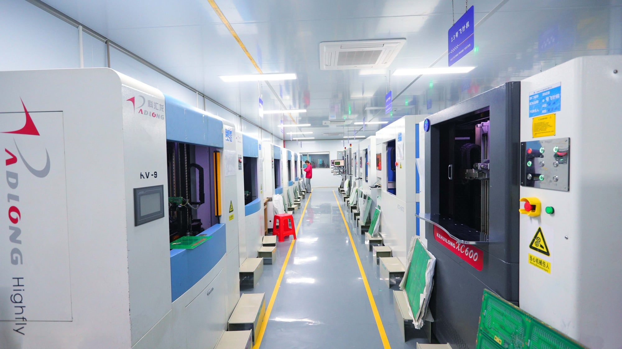
Electrical testing
Every board is tested for electrical opens and shorts before shipment. The factory has 27 flying-probe testers and three fixture testers.
Questions engineers ask us
Which Rogers materials can you build with?
We build with Rogers and other PTFE-based and ceramic-filled laminates. Tell us the exact grade and thickness when you send files and we will confirm availability and lead time.
Why use a hybrid stack-up?
Hybrid stack-ups use RF laminate only on the layers that carry RF signals and FR-4 elsewhere. That cuts material cost and makes the board easier to drill and laminate.
Can you control impedance on RF layers?
Yes. We control impedance to ±10% as standard and can tighten tolerance after reviewing your stack-up.
Send your design. Let’s build it properly.
Upload Gerber or ODB++, stack-up and quantities. Standard PCB quotes usually take 30 minutes in working hours; HDI, rigid-flex and special materials usually take up to 24 hours.