Manufacturing capabilities
These are the limits we build to on our own floor in Shenzhen. Values marked as shipped come from orders we have delivered. If your design goes beyond a value, send it anyway: many limits move with material and panel size.
Shipped in production
Board and materials
| Parameter | Capability |
|---|---|
| Layer count | 1–64 (34 shipped)Shipped in production |
| Board types | Rigid, HDI, flex, rigid-flex, metal-coreShipped in production |
| Materials | FR-4 Tg 130/150/170/180, halogen-free, IT-180, TU872, Rogers, PTFE, ceramic-filled, polyimide, aluminium, copper, CEM-1Shipped in production |
| Board thickness | 0.2–6.5 mm (6.35 mm shipped)Shipped in production |
| Maximum panel size | 609 × 889 mm |
| Minimum dielectric | 2 mil (0.05 mm) |
Drilling and plating
| Parameter | Capability |
|---|---|
| Minimum mechanical drill | 0.10 mmShipped in production |
| Minimum laser via | 0.10 mm (4 mil) |
| Plated through-hole aspect ratio | 25:1Shipped in production |
| Base copper | From 1/3 oz |
| Finished copper | Up to 8 oz |
| Via treatment | Tented, resin plugged, plugged and capped (VIPPO), copper filled |
| Back-drill | Yes |
Imaging and solder mask
| Parameter | Capability |
|---|---|
| Trace / space, inner and outer | 2/2 mil (0.05 mm); 2.6/2.6 mil in volumeShipped in production |
| Minimum annular ring | Via 3 mil, component hole 5 mil |
| BGA pitch | 0.4 mm |
| Minimum BGA pad | 8 mil |
| Solder mask bridge | 3 mil |
| Imaging | LDI for inner, outer and solder mask; film availableShipped in production |
| Solder mask colours | Green, matte green, blue, red, black, matte black, white, yellow, purple |
HDI, rigid-flex and hybrid
| Parameter | Capability |
|---|---|
| HDI structure | 1–7 steps and any-layerShipped in production |
| Microvias | Stacked or staggered, copper filledShipped in production |
| Rigid-flex | 2–16 layers |
| Hybrid RF stacks | 2–20 layers |
Finishes and special processes
| Parameter | Capability |
|---|---|
| Surface finishes | ENIG, HASL, lead-free HASL, OSP, immersion tin, immersion silver, hard gold, thick gold up to 120 µin, silver plating, ENIG + OSP, selective hard goldShipped in production |
| Special processes | Bevelled gold fingers, castellated holes, step boards, edge plating, press-fit holes |
| Impedance control | ±10% |
| Assembly services | SMT stencils and PCB assembly (PCBA) |
| Acceptance | IPC-A-600 Class 2 and Class 3; GJB military standard |
Standard tolerances
| Parameter | Capability |
|---|---|
| Outline and slots | ±0.13 mm |
| V-score position / depth | ±0.08 mm / ±0.13 mm |
| Board thickness | ±10% (±0.13 mm below 1.0 mm) |
| Plated hole diameter | ±0.075 mm |
| Non-plated hole diameter | ±0.05 mm |
| Hole position | ±0.075 mm |
| Trace width | ±20% |
| Solder mask registration | ±0.075 mm |
| Impedance | ±10%; tighter on request |
| Bow and twist | ≤0.75% (SMT boards) |
- Limits interact. For example, the smallest drill and the highest aspect ratio are not available on the same board at the same time. Our engineers confirm what applies to your design when we quote.
- Shipped values: 34 layers and 7 steps (IT-180, 6.35 mm), 2.6/2.6 mil and 0.10 mm drill (12-layer TU872 board), 120 µin gold, 159,300 holes on a P1.25 LED board.
Equipment
Main production equipment by process. Every process runs in-house, including surface finishing.
| Process | Equipment | Units |
|---|---|---|
| Imaging | LDI direct imaging (CFMEE MAS12T, Xinnuo ADI series), roller coater, automatic laminator | 7 LDI |
| Lamination | Three hot presses and one cold press, brown oxide line, X-ray and CCD target drilling | 4 presses |
| Drilling | Dongshuo CNC drills (2–6 spindle), laser drilling, CCD drilling | 26 CNC |
| Plating | Dongwei horizontal PTH, VCP via-fill and VCP pulse plating lines; Jingming pattern plating line; plasma desmear | 4 lines |
| Etching | DES (develop, etch, strip) line, copper reduction line | 2 lines |
| Solder mask | LDI solder mask exposure, low-pressure spray coaters, automatic via-plugging machines, inkjet legend printers | 4 exposure |
| Profiling | CNC routers, V-scoring, automatic gold-finger bevelling | 16 routers |
| Inspection | Inline AOI, AOI scanning and verification (incl. Orbotech), X-ray | 5 AOI |
| Electrical test | Flying-probe testers, fixture testers | 27 + 3 |
HSX / Our factory
The equipment behind the specification.
Original photographs from our Shenzhen factory. Explore the manufacturing process and the equipment used to build and inspect your boards.
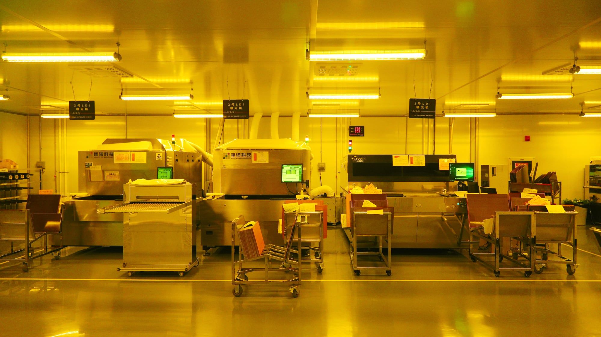
LDI imaging
Direct imaging transfers fine circuit patterns onto the panel. Inner-layer, outer-layer and solder-mask exposure are covered by our LDI equipment.
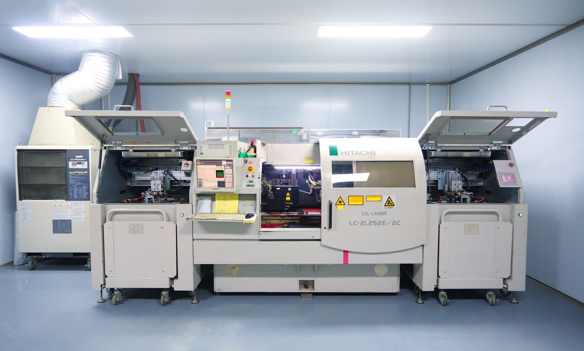
Laser drilling
Laser equipment forms the microvias used in HDI structures. Via spans and stacked or staggered construction are reviewed against the stack-up.
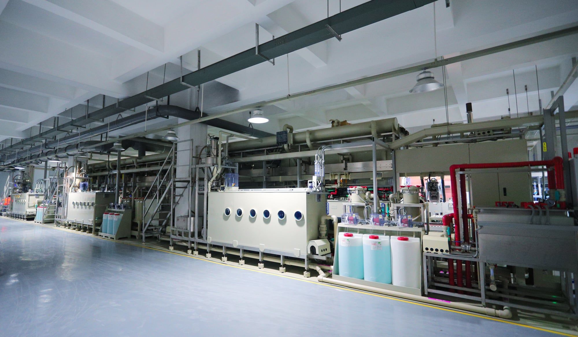
VCP copper plating
Continuous plating equipment supports the copper deposition and via-fill processes used in PCB manufacture.
Questions engineers ask us
What is your smallest trace and space?
2/2 mil (0.05 mm) on inner and outer layers. We run 2.6/2.6 mil in volume on 12-layer high-speed boards.
What is the smallest hole you can drill?
0.10 mm for both mechanical and laser drilling.
What aspect ratio can you plate?
Up to 25:1 board thickness to hole diameter, proven on a 6.35 mm, 34-layer board.
Do you build to IPC Class 3?
Yes. We build to IPC-A-600 Class 2 or Class 3 as specified on your fabrication drawing, and to the Chinese GJB military standard.
Do you offer PCB assembly and stencils?
Yes. Along with bare boards we supply SMT stencils and PCB assembly (PCBA). For an assembly quote, send the BOM and pick-and-place file with your Gerber data.
What is the largest board you can make?
The maximum working panel is 609 × 889 mm. Usable board size depends on layer count and process.
Send your design. Let’s build it properly.
Upload Gerber or ODB++, stack-up and quantities. Standard PCB quotes usually take 30 minutes in working hours; HDI, rigid-flex and special materials usually take up to 24 hours.