Heavy copper PCBs up to 8 oz
Heavy copper boards carry high current and spread heat without bus bars. We plate up to 8 oz finished copper and combine heavy copper power layers with standard signal layers in one multilayer board.
- Finished copper
- Up to 8 oz
- Base copper
- From 1/3 oz
- Edge plating
- Yes
- Finish
- ENIG, lead-free HASL, OSP
Heavy copper capability
| Finished copper | Up to 8 oz |
|---|---|
| Base copper | From 1/3 oz |
| Edge plating | Yes |
| Finish | ENIG, lead-free HASL, OSP |
How we handle heavy copper
Etch compensation
Thick copper etches with a wide foot, so spacing is compensated in CAM before imaging.
Resin fill between features
Gaps between thick copper features are filled during lamination to avoid voids and keep the surface flat for solder mask.
Edge plating
Plated board edges for shielding and grounding to the chassis.
Typical uses
- Power supplies and converters
- EV chargers
- Motor drives
- Battery management
- Industrial power
Maximum values are individual process limits, not a promise that every limit can be combined. A 34-layer, 7-step HDI board is a documented delivered build; projects above this layer count require engineering review.
Explore the builds →HSX / Our factory
The equipment behind the specification.
Original photographs from our Shenzhen factory. Explore the manufacturing process and the equipment used to build and inspect your boards.
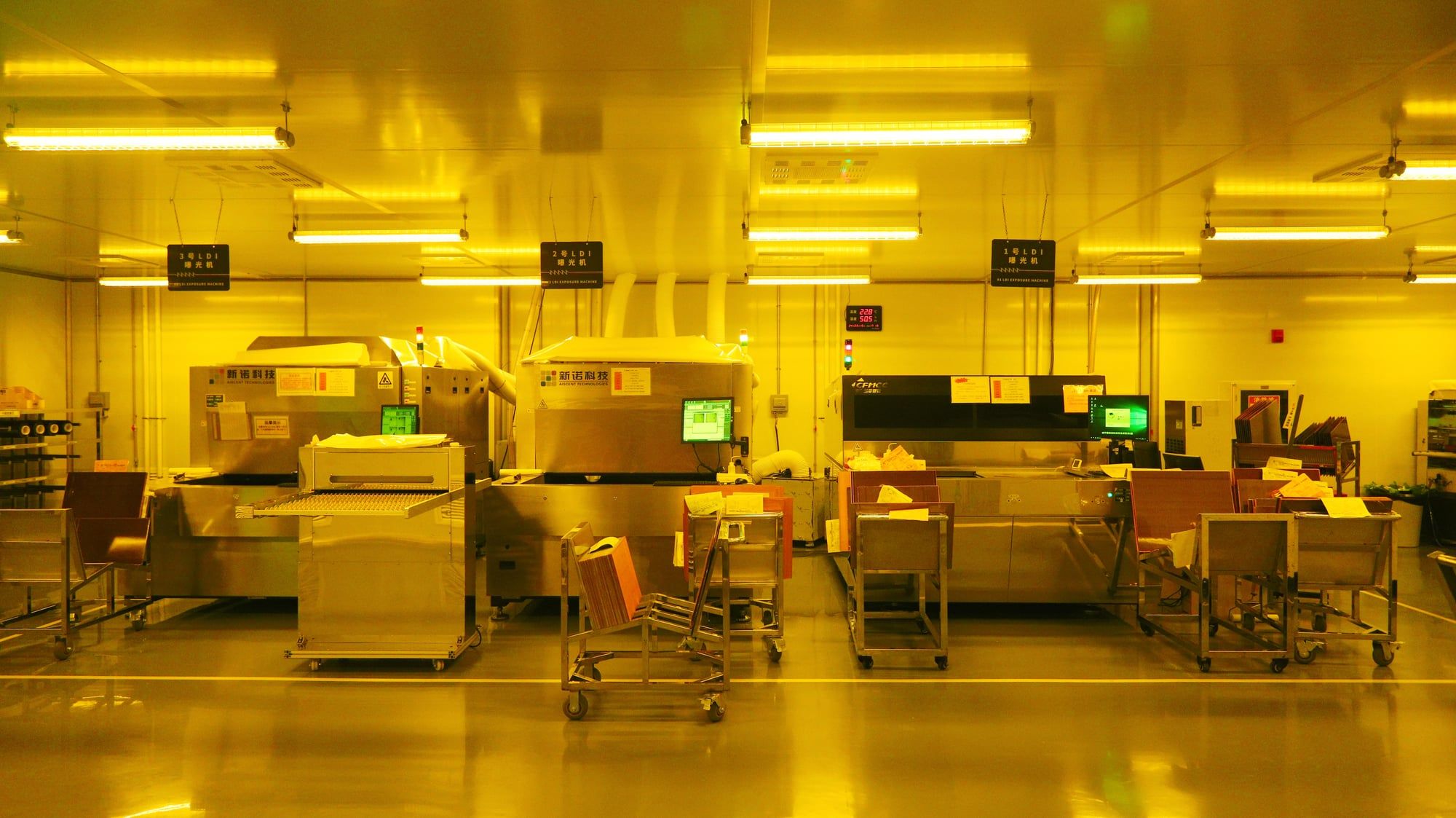
LDI imaging
Direct imaging transfers fine circuit patterns onto the panel. Inner-layer, outer-layer and solder-mask exposure are covered by our LDI equipment.
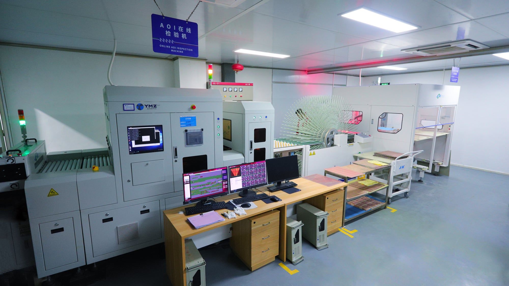
Automatic optical inspection
AOI checks circuit patterns during fabrication. Detected features are reviewed before boards continue through the process.
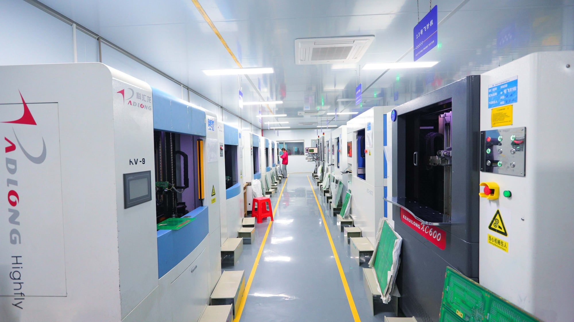
Electrical testing
Every board is tested for electrical opens and shorts before shipment. The factory has 27 flying-probe testers and three fixture testers.
Questions engineers ask us
What is the minimum spacing on 4 oz copper?
Spacing grows with copper weight because thick copper etches wider. Send us your design and we will confirm spacing per layer before quoting.
Can I mix heavy and standard copper in one board?
Yes. Power layers can be heavy copper while signal layers stay at 1/2 or 1 oz in the same stack-up.
Send your design. Let’s build it properly.
Upload Gerber or ODB++, stack-up and quantities. Standard PCB quotes usually take 30 minutes in working hours; HDI, rigid-flex and special materials usually take up to 24 hours.